EXPLORING THE TIMEX/SINCLAIR 1000'S SINCLAIR LOGIC CHIP ( SCL )
by Don Lamen, SINCUS
6-23-88
PART III, Conclusion
Note: In Part I, Nov/Dec 88, under the section titled "The SCL Chip", there is a list of circuits and/or functions af the chip. This final installment continues with (h) Internal Data Latch and goes to the conclusion. On the last page is a drawing of (f) Internal Date Bus.
Proposed Function Diagram of the ULA 2C1484E Chip - SCL
Internal Data Latch:
The Internal Data Latch is a 6 bit latch which latches in the data on Data Bus Lines D0 through D5 during Dot Cycle 3 (Code 1 AND 2 AND NOT 4). The latched data is outputted to the Address Lines A3' through A8' as part of the address to access the Dot Pattern from the ROM during Dot Cycles 6 & 7 (Code 2 AND 4).
No-Op Generator:
The No-Op Generator consists of eight inverters which forces all eight of the Data Bus Lines to 0 during Dot Cycles 4 & 5 (Code NOT 2 AND 4), just in time for the Z-80 to READ. 00000000 BINARY is the NOP instruction. This causes the microprocessor to fetch the next instruction, which is actually the next byte of data in the Data-File.
Two Shift Registers:
The Shift-Registers are alternated by bit 4 of the first counter of the Main Timing Chain (Mux Circuit). They are 8 bit shift-registers. The contents of one shift-register is being shifted out, while the other one is inhibited. When the contents of the active shift-register is shifted out the most significant bit is shifted out first and as each bit is shifted out a zero is shifted in via the serial input. The inhibited shift-register is loaded with the contents of the Data Bus during Dot Cycle 7 (Code 1 AND 2 AND 4).

- ROM/RAM SELECT CIRCUIT

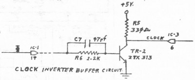
- CLOCK INVERTER BUFFER CIRCUIT

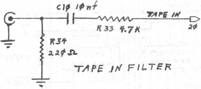
- TAPE IN FILTER
I/O Input Port FE:
The Input Port FE as far as I can tell is a 7 bit port. Bit 0 through Bit 4 monitors the keyboard. Bit 6 recieves it's input from Pin 22 (USA/UK). Bit 7 recieves it's input from Pin 20: (TAPE-IN). I have not found any use being made of Bit 5 in conjunction with Input Port FE. If Bit 5 is not used with this port then it's value should always be '1', while reading the keyboard or inputing tape data, as all Data Lines are pulled high by resistors.
Output Buffer To ROM: (ROM Driver)
The Output Buffer is a 9 Bit Tri-State Buffer which supplies part of an address to access a Dot Patern from the ROM. The rest of the address is supplied by the Microprocessor when it puts the Refresh Address on the main address lines, and comes from the Interrupt Register. The format of the whole address is:
Code: Select all
I Reg. A15-A9 Char. Code A8'-A3' Scan Count A2'-A0'
or

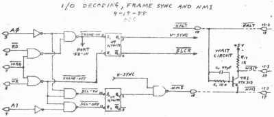
- I/O DECODING , FRAME SYNC AND NMI
I/O Decoder:
The I/O Decoder is very primitive. It samples only 5 pins; A0, A1, NOT IORQ, NOT RD, and NOT WR. It performs the following functions:
1. When A0 = 0 AND NOT RD = 0 AND NOT IORQ = 0
a) It turns on the Frame Sync Generator
b) It enables Input Port FE
c) As a result of the Frame Sync being on it holds the Scan Counter in the Reset state until the Frame Sync is turned OFF.
2. When NOT IORQ = 0 AND NOT WR = 0 any output will:
a) Turn the Frame Sync Generator OFF and release the Scan Line Counter.
b) Flash the TV screen.
3. When A0 = 0 AND NOT WR = 0 AND NOT IORQ = 0 the SCL ON-OFF Flip-Flop will be set enabling the Non-Maskable Interrupt Circuit.
4. When A1 = 0 AND NOT WR = 0 AND NOT IORQ = 0 the SCL ON-OFF Flip-Flop will be reset disabling the Non-Maskab!e Interrupt Circuit.
Non-Maskable Interrupt Generator:
The Non-Maskable Interrupt Generator consists of the SCLON-OFF Flip-Flop and a 2-input NAND gate. When the SCL ON-OFF Flip-Flop is set the NAND gate is enabled allowing the Horizontal Sync signal to pass on to Pin 15 (NOT NMI).
Wait Circuits
This circuit is outside the SCL Chip on the P. C. Board and built around transistor TR-1. When the NOT MI signal is Low and the NOT HALT Signal is High, this circuit will pull the NOT WAIT pin of the Z-80 Low generating wait states until the Horizontal Sync signal goes Low.
Frame Sync Generator:
The Frame Sync Generator is a SET-RESET Flip-Flop. It's Q output generates a signal for the Vertical Sync Pulse and goes to the Video Combiner Circuit. The NOT Q output supplies the reset for the Scan Line Counter. See I/O Decoder.
