okay, even though my interface worked, with a short program, I was worried why more signal made the loading stop working, so I made a new, much more sophisticated LTSPICE model, that generated 6 pulses ( an average between 4 and 9 pulses rounded to the nearest integer) interspersed with a low signal with a 4 pulse-width duration ( so 1200 uS, instead of 1300 uS), as a much more realistic approximation of the real TRS81 cassette signal, and I let it run for a much longer interval, so I could see what happened over longer periods.
With quite small signals all went well,but not above bout 0.4V p/p and with an about 1V p/p (peak/peak) signal I clearly saw why the load failed, the average DC level between burst kept creeping up until it ended up above the logic 1 threshold of HCT MOS, see this picture, note that red is VOUT, and green is the (partially obscured) input voltage. This means that longer and louder loads will fail!
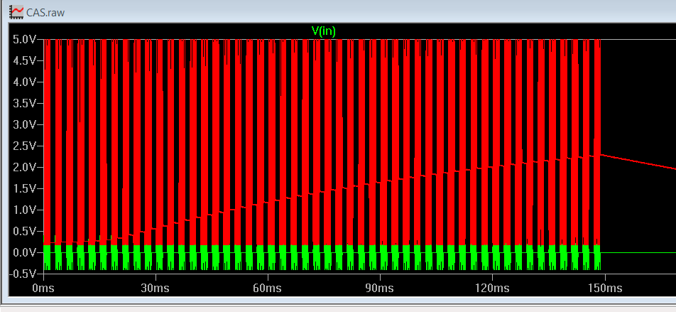
- average value after 0,15 sec with 10uF cap.png (47.87 KiB) Viewed 3526 times
so now I understand why a lower capacitor is better.
It took some experimenting with various input voltage levels, and capacitors, and after several hours I ended up with 4.7 nF as the best value!
With double that, 10nF, and loud signals the last pulse of a burst became much wider, with capacitors far below 4.7 nF, for example 0.5nF (500pF) the circuit became very insensitive 4.7 nF is the optimal value!
So here is a picture of the LTSPICE setup, and the result, showing the last pulses after a period of about 150mS (0.15s), enough to detect longer term effects:
the output signal is clean with an 1V p/p signal, but far smaller (0.3Vp/p) signals also work well, and even a 3V p/p signal works with only marginal widening of the last peak, and no "level creep up" problem, So I think I found the ideal set-up.
I also tried a permanent signal with a tenfold higher frequency to see how this circuit would cope with fast-load type of signals, and I can say it seemed to work fine.


