
16K RAM Pack Schematic / Chip Layout
Re: 16K RAM Pack Schematic / Chip Layout
1024MAK - I know what you mean about 4116's and spectrums - I've got several non-working speccy boards with 'something' (!  ) loading down the 12v line so it only gets to a few volts and kills the oscillator transistor within a few seconds -
-
1024MAK

- Posts: 5118
- Joined: Mon Sep 26, 2011 10:56 am
- Location: Looking forward to summer in Somerset, UK...
Re: 16K RAM Pack Schematic / Chip Layout
Before we get to that, I just cannot resist asking how on earth does that top RAM pack PCB stay upright, and indeed how come the Zeddy does not topple over?TMAOne wrote:My 74HCT02 chip arrived today, so I wired the circuit up, with a known good ZX81 and RAM pack.
It won't boot for me.
Admittedly, the way I've implemented it is far from elegant, but I've checked the connections and they seem to be correct. The RAMCS and A14 connections have been "broken" by using cellophane tape over the edge connector. Many of the connections at the chip are to each other, and I'd swear PokeMon even made it easy by laying out which gate to use where so that the socket pins are clustered to facilitate simply soldering them together.
Power-up only produces a white screen.
Any thoughts on how to debug?
Mark
PS I am using a smart 'phone on a train, will have a look at possible problems later...
ZX81 Variations
ZX81 Chip Pin-outs
ZX81 Video Transistor Buffer Amp
 Standby alert
There are four lights!
Step up to red alert. Sir, are you absolutely sure? It does mean changing the bulb
Looking forward to summer later in the year.
ZX81 Chip Pin-outs
ZX81 Video Transistor Buffer Amp
There are four lights!
Step up to red alert. Sir, are you absolutely sure? It does mean changing the bulb
Looking forward to summer later in the year.

Re: 16K RAM Pack Schematic / Chip Layout
Well I didn't test it, made it just up from my mind and think it should work.TMAOne wrote:My 74HCT02 chip arrived today, so I wired the circuit up, with a known good ZX81 and RAM pack.
It won't boot for me.
Admittedly, the way I've implemented it is far from elegant, but I've checked the connections and they seem to be correct. The RAMCS and A14 connections have been "broken" by using cellophane tape over the edge connector. Many of the connections at the chip are to each other, and I'd swear PokeMon even made it easy by laying out which gate to use where so that the socket pins are clustered to facilitate simply soldering them together.
Power-up only produces a white screen.
Any thoughts on how to debug?
So one further test, disconnect A14 of ram pack from the HCT02 and wire it to GND.
/RAMCS should be disconnected.
Than you have internal 1k and external no ram at all.
But the ZX81 should run (with internal RAM).
If it does, there must be an error in address decoding.
If it doesn't, there must be a hardware defect which causes system to crash without external RAM beeing addressed.
Can you do this simple test ?
Did you wire pin 14 of HCT02 to +5V and pin 7 to GND ?
Re: 16K RAM Pack Schematic / Chip Layout
I think I got it.
There has to be a diode in forward direction between pin 13 HCT02 and /ROMCS.
The HCT02 should push /ROMCS to high when A15 is high to prevent shadow copy of ROM.
But it shouldn't pull /ROMCS down (and select it) whenever A15 is low.
So there is /ROMCS and /RAMCS together selected which causes system stuck.
To prevent this you need a diode, a normal 1N4148 or similar should do the job.
Re: 16K RAM Pack Schematic / Chip Layout
Well no problem I think.1024MAK wrote: Before we get to that, I just cannot resist asking how on earth does that top RAM pack PCB stay upright, and indeed how come the Zeddy does not topple over?
Mark
The upper part of the RAM pack is connected with big hard wire which can be bended but stay always in the position and you need some power to bend them.

Re: 16K RAM Pack Schematic / Chip Layout
Still "no go".
Yes, I remembered to power the chip. I now have the 4148 in circuit. (Tried 2 different diodes, and tried reversed polarity just in case--all "no go".)
So I did "the experiment" you first thought of PokeMon. WIth A14 of the RAM pack taken to ground instead of the 74HTC02 gate output, the computer does boot with internal RAM. (That's actually 2K since this is a Timex.)
And yes Mark, lol, the wire bridge between RAM pack boards is stiff enough to hold the one board up in the air. I treat it as gently as possible, because two of my non-working (yet) packs have replacement bridges made out of old ribbon connectors. If I keep testing with this pack it's sure to break sooner or later, causing a 1/2 delay in whatever I'm doing while I fashion a replacement!
I'll stay tuned,...
Re: 16K RAM Pack Schematic / Chip Layout
What about adding buffers (and/or current limiting resistors.??) in the address and data lines, so even if there is a 'short' or other major fault in the rampack(I have a memotech one that stops a zx working regardless of how its set up/connected!), the zx will still boot up...??
Re: 16K RAM Pack Schematic / Chip Layout
Hmmm. Not sure what is exactly.TMAOne wrote: So I did "the experiment" you first thought of PokeMon. WIth A14 of the RAM pack taken to ground instead of the 74HTC02 gate output, the computer does boot with internal RAM. (That's actually 2K since this is a Timex.)
If A14 is wired to GND, the RAM pack is not selected.
If it is working on the bus, there are no possibly shortcuts.
Maybe if a chip is selected it does something wrong.
Have to look at the schematics of the RAM pack to get another idea.
Next test, what happen if you disconnect the /ROMCS connection at all ?
Does it boot ?
And another test, if you connect a correctly working ram pack with this circuit, does it boot ?
The address logic seems to be right.
Code: Select all
A15 A14      address range
0    0     => $0000-$3FFF
0    1     => $4000-$7FFF
1    0     => $8000-$BFFF
1    1     => $C000-$FFFF
Re: 16K RAM Pack Schematic / Chip Layout
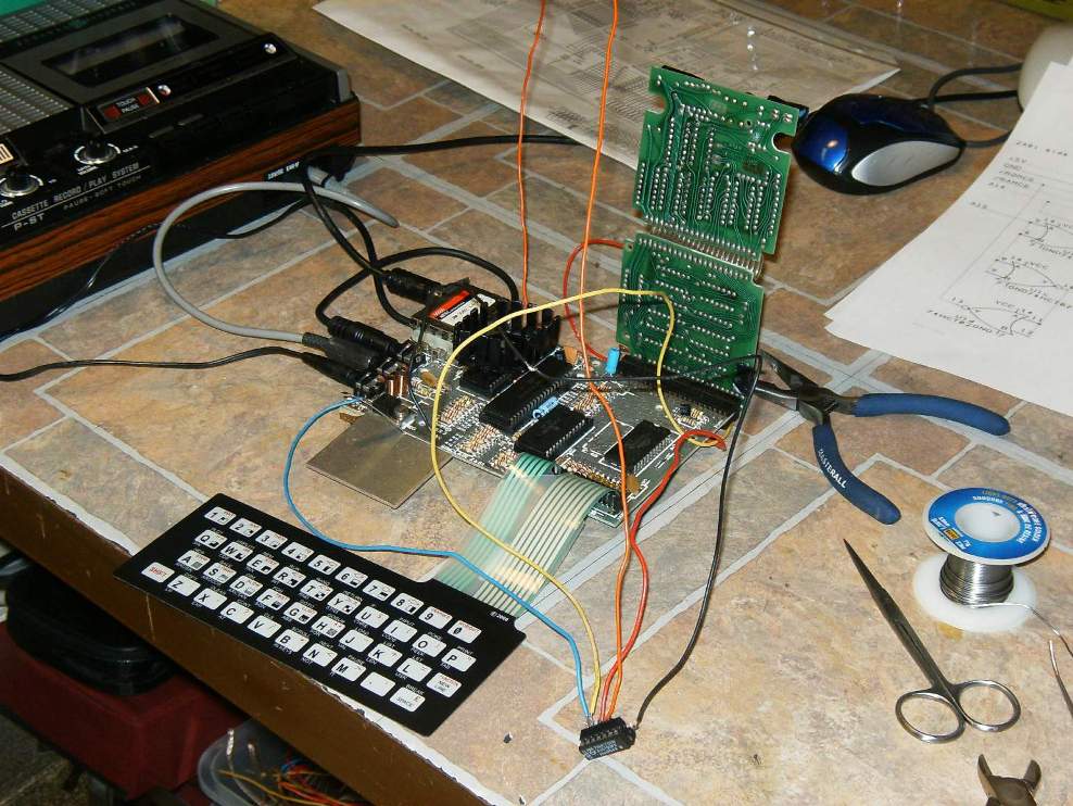
Maybe you can post a more zoomed view of your chip wiring.
As I can see on the photo you have +5V, GND and three wires.
In my schematic you need 4 additional wires:
* A14 from main board
* A15 from main board
* /ROMCS from main board
* A14 to ram pack
Can you check with a multimeter, that A14 and /RAMCS is not connected from ram pack to board to be sure ?
As I can see on the photo you have +5V, GND and three wires.
In my schematic you need 4 additional wires:
* A14 from main board
* A15 from main board
* /ROMCS from main board
* A14 to ram pack
Can you check with a multimeter, that A14 and /RAMCS is not connected from ram pack to board to be sure ?
Re: 16K RAM Pack Schematic / Chip Layout
D'oh! That's me, my bad. I got so hung up on soldering pins 5,6, 8, & 9 together I forgot to connect them to A15, then when I checked I was looking for vertical lines.PokeMon wrote:* A15 from main board
Okay, now it boots.
The RAM pack is not seen yet however. I have been using a working RAM pack for initial experiments to eliminate extraneous unknowns. POKEing 0's and 1's to 8000h PEEKs back whatever was in there before, not the value POKEd.
There is no continuity on the RAMCS or A14 connections. (The cellophane tape, which I thought would be the messiest part of this business, works amazingly well.)