Page 1 of 2
ADDRESSING RAM AT 16K+
Posted: Wed Oct 18, 2017 3:26 am
by gammaray
Ok I have been looking at the schematic for Zeddy and previous posts and cannot figure out how ANY of memory internal 1k,2k or external is addressed starting at 16K boundary.
Wouldn't A14 have to be high and ULA decide to put out a RAMCS signal to read the ghost for the RAM?
Conversely would A14 being low make ULA decide RAMCS being set inactive preventing access in 8k to 16k region?
Is this the essence of ghosting with the ULA being the decision-maker?
Re: ADDRESSING RAM AT 16K+
Posted: Wed Oct 18, 2017 10:38 am
by 1024MAK
The ULA only uses address line A14 (and the Z80 CPU control line /MREQ) to decode the control signals for the ROM and RAM.
You have to look at the address in binary:
Code: Select all
                                                      ROM RAM
Bit: 15 14 13 12 11 10  9  8  7  6  5  4  3  2  1  0  /CS /CS
====================================================  === ===
ROM   X  0  X  X  X  X  X  X  X  X  X  X  X  X  X  X   0   1  Z80 address bus
ROM   -  -  -  X  X  X  X  X  X  X  X  X  X  X  X  X   0   1  ROM chip sees this address

RAM   X  1  X  X  X  X  X  X  X  X  X  X  X  X  X  X   1   0  Z80 address bus
RAM   -  -  -  -  -  -  X  X  X  X  X  X  X  X  X  X   1   0  1k RAM chip sees this address

Where:
0 means logic zero
1 means logic one
X means 0 or 1 (either)
- means chip does not have this address bit, hence the chip ignores this signal
When ROM /CS is 0, the ROM chip is selected/enabled (activated)
When ROM /CS is 1, the ROM chip ignores the Z80 (deselected)
When RAM /CS is 0, the RAM chip is selected/enabled (activated)
When RAM /CS is 1, the RAM chip ignores the Z80 (deselected)
This means that both the ROM chip and the 1k RAM or the 2k RAM chip(s) will respond to a far greater address range than their stated capacity. Hence the same data can be read from "shadow" areas (or with RAM, written to).
If you look at the ROM address, the top three address bits are not used by the ROM (A15, A14 and A13), but the ULA uses A14 to control the ROM /CS line. So that leaves A15 and A13. Two binary digits have a range of 0 to 3, that's four combinations. Hence the ROM chip appears in the Z80 memory range (map) four times, 0x0000 to 0x1FFF, 0x2000 to 0x3FFF, 0x8000 to 0x9FFF and 0xA000 to 0xBFFF. The same happens with the RAM.
Mark
Re: ADDRESSING RAM AT 16K+
Posted: Wed Oct 18, 2017 10:58 am
by 1024MAK
Oh, and external RAM memory expansions have their own address decoder circuitry, so force the ZX81 /RAMCS ( or RAM /CS) line to logic 1 (high) to disable the ZX81's on board RAM. But because the external RAM memory expansions have a similar "incomplete" address decoder, a 16k RAM expansion will appear in the Z80 address range at both 0x4000 to 0x7FFF and at 0xC000 to 0xFFFF.
Mark
Re: ADDRESSING RAM AT 16K+
Posted: Wed Oct 18, 2017 12:26 pm
by sirmorris
That's the best explanation I've seen Mark

Re: ADDRESSING RAM AT 16K+
Posted: Wed Oct 18, 2017 4:13 pm
by 1024MAK
sirmorris wrote: ↑Wed Oct 18, 2017 12:26 pm
That's the best explanation I've seen Mark
Thank you
 Mark
Mark
Re: ADDRESSING RAM AT 16K+
Posted: Wed Oct 18, 2017 6:51 pm
by gammaray
If this schematic is accurate, there is ROMCS and A14 on ULA. So how does the ULA react when A14 is high with regards to ROMCS (assuming CPU has MEMRQ active...
I am expecting that ROMCS is an output and A14 is an "input" to ULA "asking ULA" to enable ROM.
Forcing RAMCS by external rampack does make understanding this more complicated.
They truly intended the Zeddy to be only a 16K machine. But we know better!
Re: ADDRESSING RAM AT 16K+
Posted: Wed Oct 18, 2017 7:04 pm
by 1024MAK
If you look at this schematic (where some errors have been corrected, ignore the French video circuitry) which shows the edge-connector connection points (the X's in square boxes), it may help.
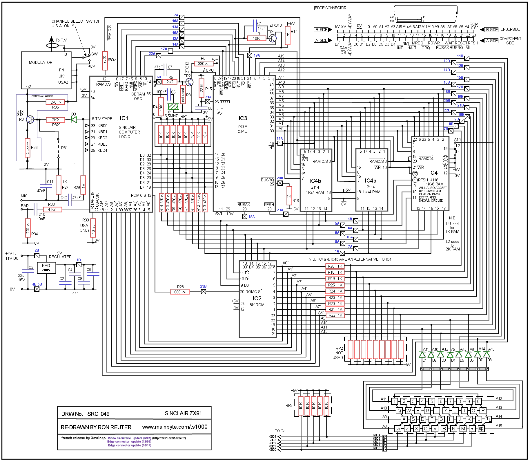 (link)
Both /ROMCS and /RAMCS have series resistors between the ULA and the relevant chips. The edge connector pins are on the memory side of the resistors. Hence why the ULA outputs can be safely overridden.
Mark
Re: ADDRESSING RAM AT 16K+
Posted: Thu Oct 19, 2017 12:56 am
by 1024MAK
gammaray wrote: ↑Wed Oct 18, 2017 6:51 pm
If this schematic is accurate, there is ROMCS and A14 on ULA. So how does the ULA react when A14 is high with regards to ROMCS (assuming CPU has MEMRQ active...
I am expecting that ROMCS is an output and A14 is an "input" to ULA "asking ULA" to enable ROM.
So, returning to this, with respect to the ULA, the A14 connection is indeed an input. /MREQ is also an input to the ULA. And both /ROMCS and /RAMCS pins are outputs. With an unexpanded ZX81, the ULA does the address decoding and controls both /ROMCS and /RAMCS so as to control the ROM and RAM chips.
As I indicated above, A14 selects whether the ROM or RAM is active. When A14 is low, the ROM is active. When A14 is high, the RAM is active.
Mark
Re: ADDRESSING RAM AT 16K+
Posted: Thu Oct 19, 2017 9:11 am
by sirmorris
On a simply expanded zeddy only the CPU drives the address lines. It doesn't _have_ to be that way but that's how it is.
Re: ADDRESSING RAM AT 16K+
Posted: Thu Oct 19, 2017 9:59 am
by siggi
1024MAK wrote: ↑Wed Oct 18, 2017 7:04 pm
If you look at this schematic (where some errors have been corrected, ignore the French video circuitry) which shows the edge-connector connection points (the X's in square boxes), it may help.
There is still an error in this schematic: At edge connector side A pin 1 should be D7
' (not D7)
Siggi