Hi Dave
First, all the DC supply voltages are within specification. For the +5V supply it should be within +/-5% or better. The minimum is 4.75V and the maximum is 5.25V.
The photos of the waveforms on your 'scope would have been more useful if you had included the range settings (volts/div and timebase setting). In my waveform pictures, because I am using a digital 'scope, you can see the settings used (this 'scope can be, and is, configured to compensate for the X10 probes, so no need to do any mental arithmetic).
Also are you using a normal 'scope probe or a switchable type set to the "X10" setting? If you have switchable probes that have a "X10" setting, please use it. You will need to calibrate the probe if you have not already done this. Also, when set to the "X10" mode, the waveform voltage displayed on the 'scope will be less by a factor of ten.
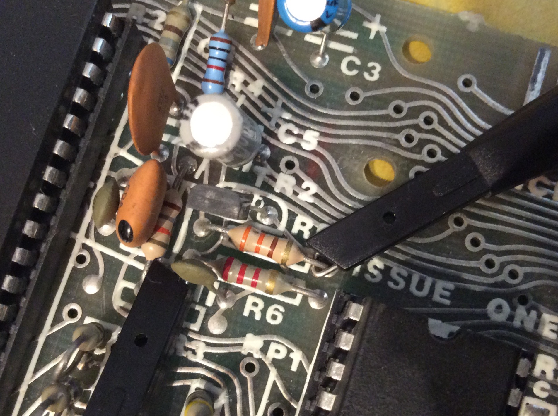
Issue 1(a)
ULA pin 14 - clock out from ULA - this looks more like what I would expect on the Z80 clock input pin (pin 6), but maybe okay. With high frequency signals, the capacitance of the 'scope and the test lead will have an effect. The effect is minimised when using X10 'scope probes.
ULA pin 16 - video out from the ULA - this is fine

Z80 pin 6 - clock input - this looks okay, assuming that the peak at the top is 4.5V or greater and that it falls to around zero at the bottom.
Issue 1(b)
ULA pin 14 - clock out from ULA - with the first photo, was the 'scope test lead ground connected properly to a ZX81 0V/GND?
ULA pin 14 - clock out from ULA - second photo. This may not look brilliant, but it is most likely okay.
ULA pin 16 - video out from the ULA - this is fine
Z80 pin 6 - clock input - it is hard to tell if this is any good.
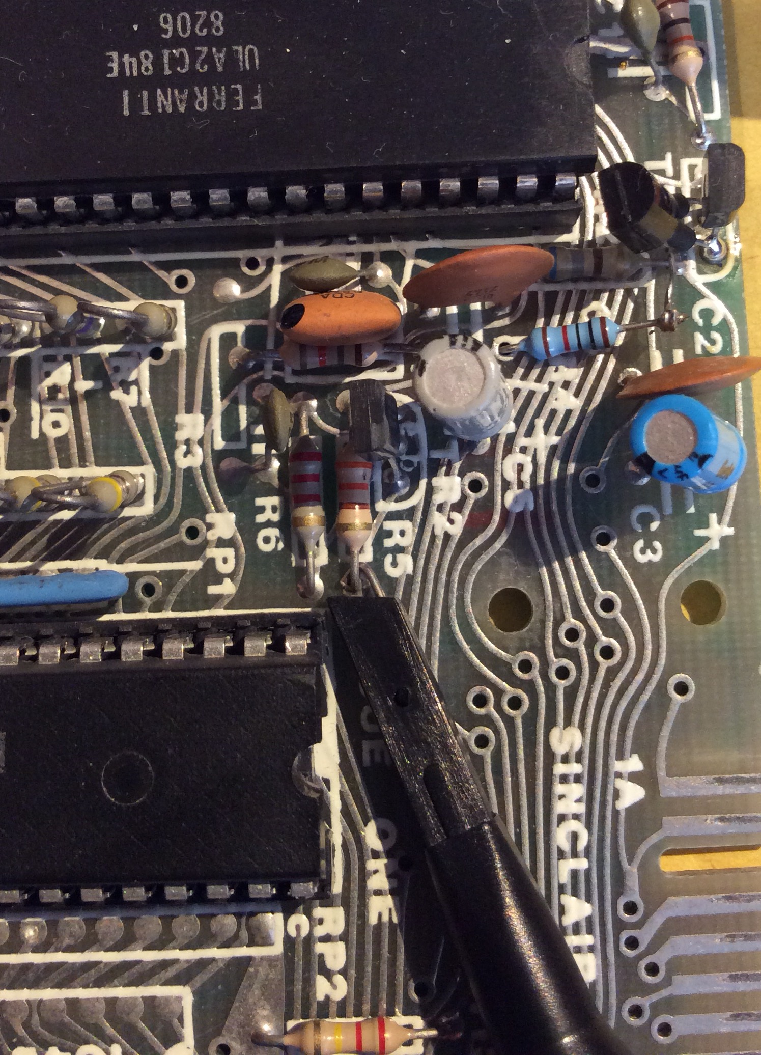
Issue 3
ULA pin 14 - clock out from ULA - it looks okay.
ULA pin 16 - video out from the ULA - this is fine
Z80 pin 6 - clock input - it is hard to tell if this is any good.
So in the hope that the CPU is getting a good clock signal, next up, to see if we can get an idea of what, if anything, it is doing.
So can you test the following CPU signals/pins:
For reference here is a pin-out of the Z80 CPU.
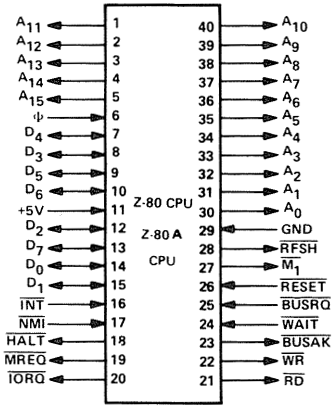
What signals do you get on the following pins of the Z80 CPU?
Be very careful, if you short the probe between adjacent pins you may damage one or more of the chips.
Pin Function
16 /INT (should be pulsing)
17 /NMI (should be pulsing)
18 /HALT (should be pulsing)
19 /MREQ (should be pulsing rapidly)
21 /RD (should be pulsing rapidly)
22 /WR (should be pulsing)
24 /WAIT (should be pulsing)
25 /BUSRQ (should be high)
26 /RESET (should be high, except for a very short time after power is applied)
27 /M1 (should be pulsing)
28 /RFSH (should be pulsing)
Then test address lines A14 and A15. These give an idea of which memory the CPU is accessing and if it is trying to generate a TV display.
You can also test the remaining address lines A0 to A13 and the data lines D0 to D7. A lack of activity is suspicious.
There is no need to take photos of all these signals if they are doing what is expected.
Mark