
A little more work, replacing "equivalent" transistors with the correct ZTX313s and finding a short now means I have three boards all showing good signals at ULA P14, TR2 and Z80 P6. Also got decent back porch at ULA p16.
On the three boards I think I have one with a good CCB Composite board, one I think I blew and one with nothing. I do have spare CCB boards which I'll add when found.
The RAM pack works. I've been touching miscellaneous pins with the oscilloscope probe and getting a constant voltage at some and squarish waves at others. But no real idea what I should be looking for.
Taking baby steps, what is the next thing I should check?
Resurrecting a ZX81 - Step by step help appreciated.
-
1024MAK

- Posts: 5118
- Joined: Mon Sep 26, 2011 10:56 am
- Location: Looking forward to summer in Somerset, UK...
Re: Resurrecting a ZX81 - Step by step help appreciated.
Okay, good progress 
I'll just refresh my memory by rereading the thread...
Mark
I'll just refresh my memory by rereading the thread...
Mark
ZX81 Variations
ZX81 Chip Pin-outs
ZX81 Video Transistor Buffer Amp
 Standby alert
There are four lights!
Step up to red alert. Sir, are you absolutely sure? It does mean changing the bulb
Looking forward to summer later in the year.
ZX81 Chip Pin-outs
ZX81 Video Transistor Buffer Amp
There are four lights!
Step up to red alert. Sir, are you absolutely sure? It does mean changing the bulb
Looking forward to summer later in the year.
-
1024MAK
- Posts: 5118
- Joined: Mon Sep 26, 2011 10:56 am
- Location: Looking forward to summer in Somerset, UK...
Re: Resurrecting a ZX81 - Step by step help appreciated.
Hi Dave
I presume you have confirmed that the RAM pack is working okay with a working ZX81?
Now that the CPU on each board is getting a good clock signal, next up, to see if we can get an idea of what, if anything, they are doing.
So, for each board can you test the following CPU signals/pins:
For reference here is a pin-out of the Z80 CPU.
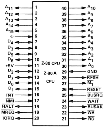
What signals do you get on the following pins of the Z80 CPU?
Be very careful, if you short the probe between adjacent pins you may damage one or more of the chips.
Remember, we are just looking to see which lines are active, don't worry about the actual waveform.
Pin Function
16 /INT (should be pulsing)
17 /NMI (should be pulsing)
18 /HALT (should be pulsing)
19 /MREQ (should be pulsing rapidly)
21 /RD (should be pulsing rapidly)
22 /WR (should be pulsing)
24 /WAIT (should be pulsing)
25 /BUSRQ (should be high)
26 /RESET (should be high, except for a very short time after power is applied)
27 /M1 (should be pulsing)
28 /RFSH (should be pulsing)
Then test address lines A14 and A15. These give an idea of which memory the CPU is accessing and if it is trying to generate a TV display.
You can also test the remaining address lines A0 to A13 and the data lines D0 to D7. A lack of activity is suspicious.
There is no need to take photos of all these signals if they are doing what is expected.
How many channels does your 'scope have? One or two? Does it have a separate sync input?
Mark
I presume you have confirmed that the RAM pack is working okay with a working ZX81?
Now that the CPU on each board is getting a good clock signal, next up, to see if we can get an idea of what, if anything, they are doing.
So, for each board can you test the following CPU signals/pins:
For reference here is a pin-out of the Z80 CPU.
What signals do you get on the following pins of the Z80 CPU?
Be very careful, if you short the probe between adjacent pins you may damage one or more of the chips.
Remember, we are just looking to see which lines are active, don't worry about the actual waveform.
Pin Function
16 /INT (should be pulsing)
17 /NMI (should be pulsing)
18 /HALT (should be pulsing)
19 /MREQ (should be pulsing rapidly)
21 /RD (should be pulsing rapidly)
22 /WR (should be pulsing)
24 /WAIT (should be pulsing)
25 /BUSRQ (should be high)
26 /RESET (should be high, except for a very short time after power is applied)
27 /M1 (should be pulsing)
28 /RFSH (should be pulsing)
Then test address lines A14 and A15. These give an idea of which memory the CPU is accessing and if it is trying to generate a TV display.
You can also test the remaining address lines A0 to A13 and the data lines D0 to D7. A lack of activity is suspicious.
There is no need to take photos of all these signals if they are doing what is expected.
How many channels does your 'scope have? One or two? Does it have a separate sync input?
Mark
ZX81 Variations
ZX81 Chip Pin-outs
ZX81 Video Transistor Buffer Amp
Standby alert
There are four lights!
Step up to red alert. Sir, are you absolutely sure? It does mean changing the bulb
Looking forward to summer later in the year.
ZX81 Chip Pin-outs
ZX81 Video Transistor Buffer Amp
There are four lights!
Step up to red alert. Sir, are you absolutely sure? It does mean changing the bulb
Looking forward to summer later in the year.
Re: Resurrecting a ZX81 - Step by step help appreciated.
Hi Mark,
Im going to post a couple of pics to make sure I know what pulse/rapid pulse etc looks like:

normal pulse eg Z80 Pin 16 .5us 5V

rapid pulse eg Z80 Pin 19 .5us 5V

Address pin

ROM line
Results when testing gave
Pin Function
PULSE 16 /INT (should be pulsing)
5V 17 /NMI (should be pulsing)
0V 18 /HALT (should be pulsing)
RAPID 19 /MREQ (should be pulsing rapidly)
RAPID 21 /RD (should be pulsing rapidly)
PULSE 22 /WR (should be pulsing)
5V 24 /WAIT (should be pulsing)
5V 25 /BUSRQ (should be high)
5V ok 26 /RESET (should be high, except for a very short time after power is applied)
PULSE 27 /M1 (should be pulsing)
PULSE 28 /RFSH (should be pulsing)
So it looks like /NMI is getting held high, /HALT low and /WAIT high.
Other info, my scope is a Farnell DVT 60 with 2 channels and a load of switches. There is a 3rd channel but just a vertical adjustment and connector.
Im not sure about separate sync input, but I could read the manual...
Im going to post a couple of pics to make sure I know what pulse/rapid pulse etc looks like:
normal pulse eg Z80 Pin 16 .5us 5V
rapid pulse eg Z80 Pin 19 .5us 5V
Address pin
ROM line
Results when testing gave
Pin Function
PULSE 16 /INT (should be pulsing)
5V 17 /NMI (should be pulsing)
0V 18 /HALT (should be pulsing)
RAPID 19 /MREQ (should be pulsing rapidly)
RAPID 21 /RD (should be pulsing rapidly)
PULSE 22 /WR (should be pulsing)
5V 24 /WAIT (should be pulsing)
5V 25 /BUSRQ (should be high)
5V ok 26 /RESET (should be high, except for a very short time after power is applied)
PULSE 27 /M1 (should be pulsing)
PULSE 28 /RFSH (should be pulsing)
So it looks like /NMI is getting held high, /HALT low and /WAIT high.
Other info, my scope is a Farnell DVT 60 with 2 channels and a load of switches. There is a 3rd channel but just a vertical adjustment and connector.
Im not sure about separate sync input, but I could read the manual...
-
1024MAK
- Posts: 5118
- Joined: Mon Sep 26, 2011 10:56 am
- Location: Looking forward to summer in Somerset, UK...
Re: Resurrecting a ZX81 - Step by step help appreciated.
Hmm. Well at least we know the CPU is trying to do some memory activity. HALT should not be low all the time. That's very odd.
/NMI and /WAIT may well be high if the CPU is not correcty running the code from the ROM.
Mark
 Just a reminder to myself that I have more to add later.
/NMI and /WAIT may well be high if the CPU is not correcty running the code from the ROM.
Mark
ZX81 Variations
ZX81 Chip Pin-outs
ZX81 Video Transistor Buffer Amp
Standby alert
There are four lights!
Step up to red alert. Sir, are you absolutely sure? It does mean changing the bulb
Looking forward to summer later in the year.
ZX81 Chip Pin-outs
ZX81 Video Transistor Buffer Amp
There are four lights!
Step up to red alert. Sir, are you absolutely sure? It does mean changing the bulb
Looking forward to summer later in the year.
-
1024MAK
- Posts: 5118
- Joined: Mon Sep 26, 2011 10:56 am
- Location: Looking forward to summer in Somerset, UK...
Re: Resurrecting a ZX81 - Step by step help appreciated.
So, when the CPU executes a HALT instruction, it stops getting new instructions from memory and instead does NOP (no operation) cycles. This maintains the the CPU bus signals including the memory refresh signals (important for DRAM).
The CPU will not do anything else until either it is reset, or an interrupt is received (/INT or /NMI). In your post where you report the state of the CPU signals, /INT is listed as pulsing, but /HALT is listed as 0V. Oh, and yes you get the idea between the different pulses that are expected.
So there are a number of possibilities that may cause this strange state. One is that /HALT is pulsing high occasionally, but very quickly and it was not seen on the 'scope. Another is that the data read from the memory by the CPU is garbage (so the CPU is seeing more HALT instructions than it should do), and the third is that the CPU is faulty (or it never got a proper reset pulse).
Damage (break/crack) to the PCB tracks, poor edge-connector contact, or a short caused by a solder splash, or defective RAM, or a faulty ROM all could be the cause of the CPU getting garbage data during a memory read.
You could do the test again and see if the results are the same again, or if they are different.
Mark
ZX81 Variations
ZX81 Chip Pin-outs
ZX81 Video Transistor Buffer Amp
Standby alert
There are four lights!
Step up to red alert. Sir, are you absolutely sure? It does mean changing the bulb
Looking forward to summer later in the year.
ZX81 Chip Pin-outs
ZX81 Video Transistor Buffer Amp
There are four lights!
Step up to red alert. Sir, are you absolutely sure? It does mean changing the bulb
Looking forward to summer later in the year.

Re: Resurrecting a ZX81 - Step by step help appreciated.
Did you already change the ULA ?
Keeping in HALT results easily if a HALT instruction is executed when no NMI is present. Too bad - can be a faulty ROM as well. Isn't it possible to check this with a ZXpand while providing it's own ROM ? Just an idea - not sure if you have a ZXpand in your fridge.
I got this error (stuck in HALT) whenever I missprogrammed my ZXmore or ZXblast firmware while executing accidently HALT with NMI off. This is a killer and the system is stuck forever.