Page 6 of 7
Re: Help in resurrecting my ZX81
Posted: Sun Aug 19, 2018 7:39 pm
by Andy Rea
yeah i dont think my brain is operating correctly... the 2K2 resistor... if you have something one side and nothing the other then the nothing side must be shorted.
Andy
Re: Help in resurrecting my ZX81
Posted: Sun Aug 19, 2018 7:48 pm
by Paul
Did you measure that the resistance is still 2k2?
Re: Help in resurrecting my ZX81
Posted: Sun Aug 19, 2018 8:32 pm
by mrtinb
Andy Rea wrote: ↑Sun Aug 19, 2018 4:42 pm
i would pull TR2 and then see what you get at the base connection.
I've removed the transistor TR2. (Which for me is a little difficult without a desolder gun.)
These are the values without TR2:
Code: Select all
...............................
:            :  Broken ZX81   :
:            : with Andys ULA :
:            :  without TR2   :
:............:................:
: ULA pin 14 :          1.510 :
: R6 2K2 in  :          1.510 :
: R6 2K2 out :          1.590 :
: TR2 in     :          1.590 :
: TR2 out    :          0.000 :
:............:................:
Re: Help in resurrecting my ZX81
Posted: Mon Aug 20, 2018 12:44 pm
by 1024MAK
ZX81 clock circuit operation
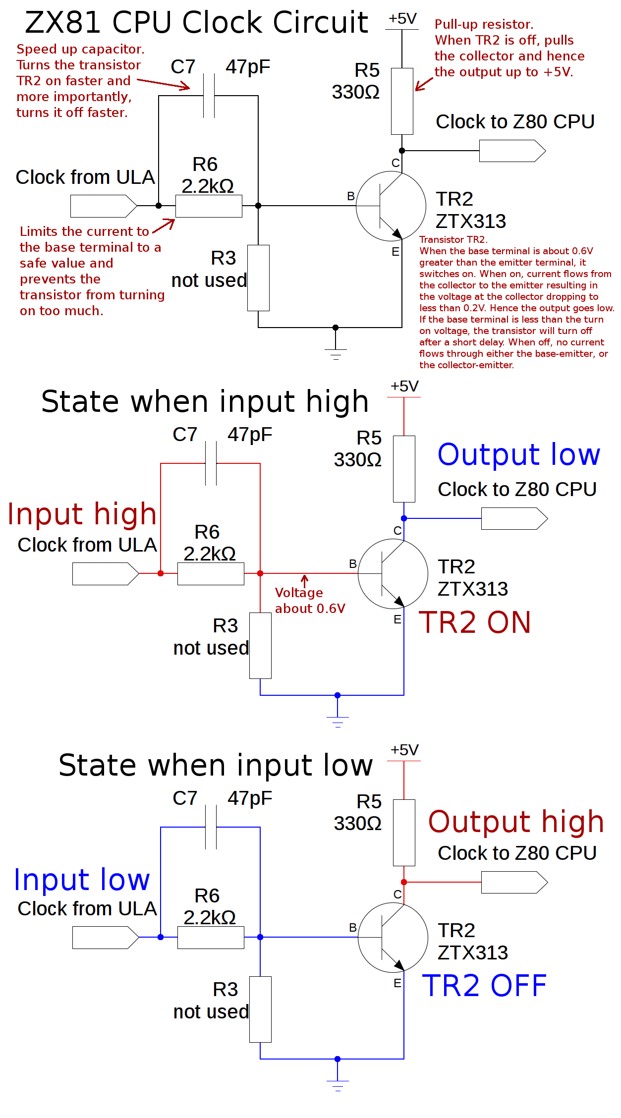
Please note that the coloured circuit states shown in the diagram are true only during the stable part of the signal from the ULA clock output pin, or when the circuit is static. By static, I mean the input is DC and not a high frequency signal.
In reality, when the ULA clock output pin is changing state from high to low, TR6 will stay on for a short time even though it's base voltage has dropped below it's turn on voltage (approx 0.6V). Note that this voltage of 0.6V is the DC value. If measured by a multimeter in a live circuit running at 3.25MHz, the meter will indicate a lower voltage.
The speed up capacitor briefly allows a greater current to flow from the ULA output to the transistors base terminal (when the ULA output goes from low to high) to switch the transistor on faster. This aids in making the output at the collector a nicer, cleaner "square wave edge". When the output from the ULA goes from high to low, the speed up capacitor allows current to briefly flow from the transistors base to ground via the capacitor and the output stage of the ULA. Hence helping to remove charge from the base area of the transistors semiconductor. This aids in getting the transistor to switch off quicker.
The speed that the transistor switches is important. If it takes too long to switch off, by the time the collector and hence the output has changed,the input signal may have already changed logic state again. Then the Z80 clock pin would not see a changing signal, but instead just see a continuous logic low signal.
Mark
Re: Help in resurrecting my ZX81
Posted: Mon Aug 20, 2018 1:31 pm
by 1024MAK
mrtinb wrote: ↑Sun Aug 19, 2018 8:32 pm
Andy Rea wrote: ↑Sun Aug 19, 2018 4:42 pm
i would pull TR2 and then see what you get at the base connection.
I've removed the transistor TR2. (Which for me is a little difficult without a desolder gun.)
These are the values without TR2:
Code: Select all
...............................
:            :  Broken ZX81   :
:            : with Andys ULA :
:            :  without TR2   :
:............:................:
: ULA pin 14 :          1.510 :
: R6 2K2 in  :          1.510 :
: R6 2K2 out :          1.590 :
: TR2 in     :          1.590 :
: TR2 out    :          0.000 :
:............:................:
With TR2 removed from the PCB, the clock input pin (6) on the Z80 CPU should be pulled high to +5V by R5. As the collector PCB pad should be connected to R5 and to pin 6 of the Z80 CPU, this should also be at +5V.
Mark
Re: Help in resurrecting my ZX81
Posted: Mon Aug 20, 2018 3:03 pm
by mrtinb
It seems the reason for this complex circuit is to make an inverse clock on the CPU.

Why aren't they just similar, and run the same heart beat?
Re: Help in resurrecting my ZX81
Posted: Mon Aug 20, 2018 3:35 pm
by 1024MAK
The reason for using a transistor in this way is to meet the requirements specified by Zilog for the input to the clock pin on the Z80 CPU. The ULA on it's own could not produce the correct logic levels to meet these requirements.
Mark
Re: Help in resurrecting my ZX81
Posted: Mon Aug 20, 2018 4:20 pm
by 1024MAK
Attached are two extracts from Zilog documents giving details about the clock input.
If you compare the clock input voltages (VILC and VIHC) to the normal logic pin input voltages (VIL and VIH) you will see that they have to get much closer to the VCC (+5V) supply and to GND (0V) than the normal logic pin inputs.
Mark
Re: Help in resurrecting my ZX81
Posted: Sun Sep 02, 2018 2:32 pm
by mrtinb
I have measured wrong on the circuit, and updated the drawing.
Edit: This drawing is also wrong. I'll continue to measure.

Re: Help in resurrecting my ZX81
Posted: Tue Jan 01, 2019 9:27 pm
by mrtinb
So this thread has been cold for a while. I had to lay it aside, as it was getting very irritating.
Now I finally got my other hardware project working, a TZXduino, so I can load programs into my Lambda 8300. (See picture 1)
I now got the courage to get back to the troublesome Zeddy board.
We left of trying to see where the clock signal from the ULA was lost. Let's start where the clock signal starts: At the ULA pin 14.
The question is: Knowing that the DSO138 oscilloscope cannot measure the speed of the Zeddy, shouldn't some of the samples be at 0V and not as here a constant power of 1.5V?
(Picture 1)

(Picture 2)
