Page 1 of 3
ZX81 Chip Pin-outs
Posted: Sun Nov 24, 2013 11:23 am
by 1024MAK
Re: ZX81 Chip Pin-outs
Posted: Sun Nov 24, 2013 11:32 am
by 1024MAK
Sinclair ZX81 ULA
Code: Select all
ZX81 Ferranti ULA
Pin  Function  Function  Pin
 1   A7'         +5V     40
 2   A8'         A6'     39
 3   A2'         A5'     38
 4   A1'         A4'     37
 5   A0'         A3'     36
 6   /RD         OSC     35
 7   /IORQ       GND     34
 8   /WR         KBD0    33
 9   /MREQ       D0      32
10   /M1         KBD1    31
11   A14         D1      30
12   /RAMCS      KBD2    29
13   /ROMCS      D2      28
14   /CLK (CPU)  KBD3    27
15   /NMI        D3      26
16   TV/TAPE     KBD4    25
17   /HALT       D4      24
18   A15         D5      23
19   D7          USA/UK  22
20   TAPE IN     D6      21
I hope these pin-outs are helpful to those who do not yet have this information etched in to their minds yet

If you spot any errors, please let me know so that I can correct them.
Also note that the ROM socket and RAM socket may be bigger than the size of the chip actually fitted. These pin-outs are for the chips, not the sockets.
1 bit X 16k 4116 DRAM
As used in both Sinclair's 16k byte RAM pack and many other 16k byte RAM expansions.
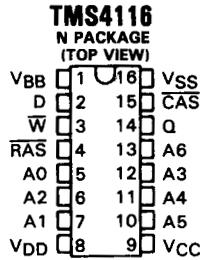
- 4116 DRAM pin-out
- 4116 DRAM pin-out_p.png (35.44 KiB) Viewed 25577 times
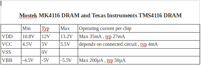
- 4116 DRAM voltages and currents
- 4116 current_p.png (21.25 KiB) Viewed 25577 times
Mark
Re: ZX81 Chip Pin-outs
Posted: Sun Nov 24, 2013 4:11 pm
by Rink
Never come across PSRAM before - looks cool. Anyone know where you can buy it?
I hate DRAM, but find the capacities of SRAM to be quite disappointing so this stuff looks interesting.
Re: ZX81 Chip Pin-outs
Posted: Sun Nov 24, 2013 10:24 pm
by sirmorris
Great stuff, Mark! Thanks

Re: ZX81 Chip Pin-outs
Posted: Sun Nov 24, 2013 10:43 pm
by yalokinh
Great, thanks
Re: ZX81 Chip Pin-outs
Posted: Wed Nov 27, 2013 4:48 pm
by yalokinh
For the 2114, i think there are two of them, do the pins for both chips go to the same place?
Re: ZX81 Chip Pin-outs
Posted: Wed Nov 27, 2013 4:58 pm
by PokeMon
As for the RAMs the address lines and data lines can be swapped in any way, you can not trust that A5 goes to A5 or that I/O3 goes to D3 or D4.
Re: ZX81 Chip Pin-outs
Posted: Wed Nov 27, 2013 6:34 pm
by 1024MAK
yalokinh wrote:For the 2114, i think there are two of them, do the pins for both chips go to the same place?
If you are using 2114 SRAM chips, two are needed. One does 4 bits of the 8 bit byte, the other does the remaining 4 bits of the byte. Connect the ten address lines of both to the A0 - A9 address lines of the Z80 CPU.
As PokeMon says, the actual order of the connections is not important. What do we mean by this? Well, as the Z80 writes data to the RAM , and the RAM does not care where that data is stored, it makes no difference if the address lines are mixed up. For example you can route Z80 CPU A0 to RAM A2, CPU A1 to RAM A1, CPU A3 to RAM A0, CPU A4 to RAM A3 etc. as long as all the address lines connect to the "lower" address lines (A0 - A9) of the CPU.
You can do the same for the data lines (CPU D0 - D7) to the RAM I/O1 - I/O4. Route four of the data lines (CPU D0 - D7) to the I/O pins of one 2114, and route the remaining data lines to the second 2114 chip
Note that the ULA named pins do have to tie up with ("connect with" either directly or via the resistors) the similar named Z80 CPU pins as per the schematic diagram.
The system will work fine, as the CPU can read and write data to the RAM.
Note this mixed up connection system will not work for the ROM. It only works for static RAM chips.
Mark
Edited to add a word that I missed out (work) in the last sentence

Re: ZX81 Chip Pin-outs
Posted: Thu Nov 28, 2013 2:35 am
by yalokinh
ah cool, learning lots!
Thanks