Page 3 of 3

Re: ZX81 Chip Pin-outs

Posted: Tue Apr 11, 2017 1:33 am
by 1024MAK
2016 / 6116 and 62256 SRAM pin-outs added to my earlier post.

Mark

Re: ZX81 Chip Pin-outs

Posted: Tue Apr 11, 2017 8:14 am
by povvercrazy
Awesome job Mark thank you for adding those, I will now treat all address lines on pinouts as A'n' and not a specific number, its greatly helped my understanding.

Re: ZX81 Chip Pin-outs

Posted: Tue Apr 11, 2017 11:52 am
by 1024MAK
Pin details on the CPU will always be correct.
With most systems, pin details on ROM chips will be correct.
The pin out for the ZX81 ULA is (I hope) correct.

It's just RAM chips on the Zeddy that you have to watch out for...

Mark

Re: ZX81 Chip Pin-outs

Posted: Mon Nov 09, 2020 10:52 pm
by bola_dor
I know I am resurrecting a zombie here but this post is used frequently as reference.

As discussed earlier RAM implementation can use Address and Data lines in any order disregarding the original labeling.
I had a hard time testing an ISSUE 3 ZX81 (red) board from a TS1000 found in a CZ1000 (it has R30 cutted off) because I tried to check continuity using the original pinout as found in every datasheet and in this post.
So, This is how I finally found IC4 is connected in this particular board. (I don't know IF this is true for an ISSUE 1 board).
This is for the big IC 4 ram chip . In my case a 2Kb model.. I guess IC 4a/b have all lines scrambled also...
CZ1000 RAM .jpg

ZX81 ROM Socket pin out and 2764 EPROM pin out

Posted: Thu Nov 18, 2021 12:23 am
by 1024MAK
ZX81 ROM Socket pin out and 2764 EPROM pin out
Note that in the above diagram, "ZX81 PCB" means the socket pin.
"Mask ROM" means an original 24 pin plastic Sinclair ROM chip (the type without a window on top).

If a 2764, 27C64, 27128 , 27C128, 27256 or 27C256 EPROM is being used, some wiring changes are needed.

Pins 1 through to 19 are okay as is.

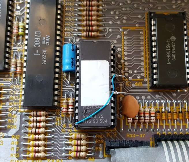
EPROM chip pin 20 needs to be bent up so it does not enter the socket.
Use a thin insulated solid core wire to link EPROM chip pins 14 (GND) and 20.

Pins 21 and 22 are okay.

EPROM chip pin 23 needs to be bent up so it does not enter the socket.
Use a thin insulated solid core wire to link EPROM chip pin 23 (A11) to socket pin 20 (A11).

Pins 24 through to 28 are okay as is.

If a 27128 or 27C128 EPROM is being used, the ROM image (data) must be programmed to start at chip address 0x2000 (8192). In other words, it must be programmed in the upper half of the chip.

If a 27256 or 27C256 EPROM is being used, the ROM image (data) must be programmed to start at chip address 0x6000 (24576). In other words, it must be programmed in the top quarter of the chip.

Here's a photo showing the modification:
Image

See this topic for the source of the photo.

Mark

Re: ZX81 Chip Pin-outs

Posted: Tue Nov 08, 2022 9:01 am
by XavSnap
64K.jpg
eprom[1].jpg
infocarte[1].jpg

Tableau des brochages des EPROM v200.pdf
(428.71 KiB) Downloaded 115 times

Re: ZX81 Chip Pin-outs

Posted: Tue Nov 08, 2022 10:43 am
by 1024MAK
Nice 8-). Do you want to attach a copy of your Inboard 64K RAM Decoder diagram as a zip, so we can get a higher quality copy?

Mark

Re: ZX81 Chip Pin-outs

Posted: Tue Nov 08, 2022 2:23 pm
by XavSnap

Re: ZX81 Chip Pin-outs

Posted: Wed Nov 09, 2022 8:15 am
by XavSnap