Houston, we have an image!

Any discussions related to the creation of new hardware or software for the ZX80 or ZX81
User avatar
PokeMon
Posts: 2264
Joined: Sat Sep 17, 2011 6:48 pm

Re: Houston, we have an image!

Post by PokeMon »

Andy Rea wrote:Well now i'm really baking my noodle, how the blinkin heck does 1K hi-res work ! it looks to me that during refresh, ramcs is low when mreq is low then you get 1/2 cycle of romcs for the last half of T4....

However thinking about it nearly every hi-res enabled ram expansion also uses refresh signal and rd to enable ram... which ties in nicely with all this romcs strecthing... there is always something new to learn :)
Seems that maybe this is my problem when enabling /RD with /RFSH.
But /CS is only active low when A14 or A15 high which couldn't be during normal video execution, couldn't it ? :o
User avatar
PokeMon
Posts: 2264
Joined: Sat Sep 17, 2011 6:48 pm

Re: Houston, we have an image!

Post by PokeMon »

Now found picture here:
http://searle.hostei.com/grant/zx80/zx80ScopePics.html

Does anybode know, why ROMCS is stretched during video execution ?
I override the ROMCS and just enable it when A14 and A15 is low.
This does work fine when not enabling RAM during refresh.
The problem is independent if I override the ROMCS or not.

So it's maybe not important if ROMCS is stretched ? :?
User avatar
RetroTechie
Posts: 379
Joined: Tue Nov 01, 2011 12:16 am
Location: Hengelo, NL
Contact:

Re: Houston, we have an image!

Post by RetroTechie »

Hi PokeMon,

Have you checked documentation with my ZX81 ULA project? There's a similar 'scope' picture in it which may explain a lot:
Signal_timing.png
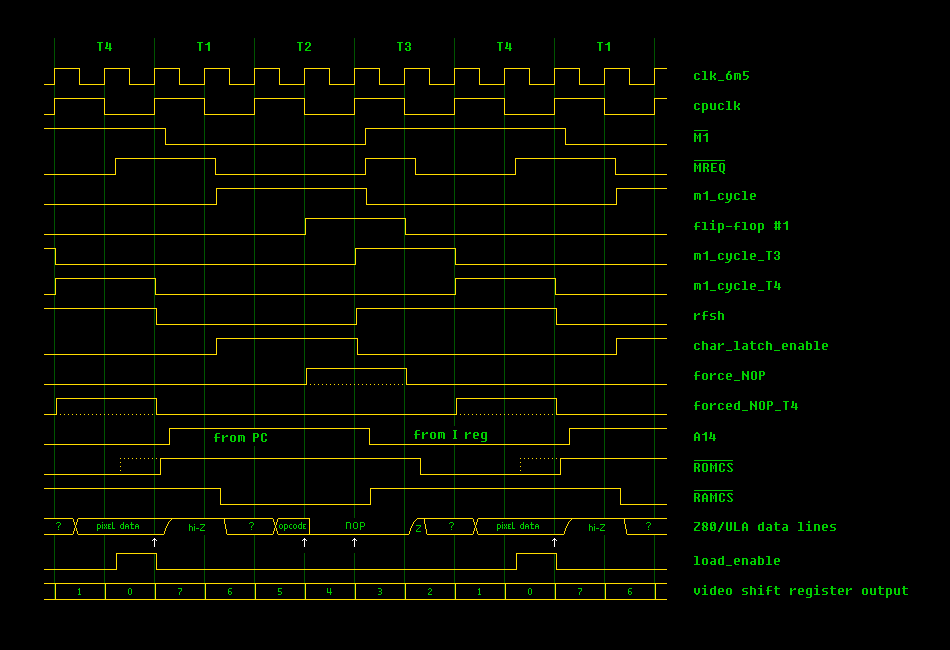
Signal_timing.png (4.09 KiB) Viewed 2747 times
What version ULA do you have? What are you using as RAM (internal or RAM pack), and what's the logic for control signals? Do you experience same problems with regular ZX81 display, pseudo hi-res and true hi-res software?

First thing to realize is there are 2 stages in DFILE execution: 1) The instruction fetch (where Z80 gets fed a NOP), and 2) The refresh cycle that follows (where either ROM or RAM outputs the graphic data).

The instruction fetch is basically a regular memory read, where A14/A15 determine source of the data. But in a refresh cycle, I register is on high bits of the address bus. That tidbit of info is HARD to find :x in official docs, but here it is: quoting the MK3880 Technical Manual, /RFSH pin description:
A7 is logic zero and the upper 8 bits of the Address Bus contains the I Register.
First part of that statement is probably not true; R register is on A0-A7, bit 7 of that is usually 0 (=reset state, and isn't included in refresh counter), but programmer can set it using LD R,A instruction, and that bit is preserved (as expected).
Second half of above quote is true AFAIK.
PokeMon wrote:I heard about stretched /ROMCS.
Could anybode explain more in detail ?
In normal ROM reads, /ROMCS follows /MREQ timing. In DFILE execution (refresh cycle), /ROMCS activates when /MREQ goes active, but stays active after /MREQ returns to inactive (see dotted part in above picture). As far as I (or Grant) know, only for forced NOP cycles (DFILE execution), not regular refresh cycles or memory read/writes.

Why? IMHO: simply to accomodate a convenient point in time to clock ULA's video shift register. Read: a point in time which allows you to clock that data directly, in such a way that all pixels get equal 'display time' when shifted out to the screen, and without tricks like an extra 8-bit buffer or 9th bit in between. Which is the exact same reason I'm duplicating that /ROMCS behavior in my ZX81 ULA project.
So it's maybe not important if ROMCS is stretched ? :?
Purely an implementation issue, not something that "should be done". As long as net effect is the same, anything goes.
Sometimes "K" appears, sometimes software crashes when pressing any key.
That's an important observation! If the wrong graphic data is fetched by the ULA, it does not affect CPU operation, and you'd see screen corruption but stable running machine. So if you experience crashes, that would suggest something goes wrong during the instruction fetch (and following from that, maybe wrong character code gets clocked into the ULA's character latch, which might explain "K" cursor corruption).

There's a few things to check:
  • Regardless of what control signals you input, /ROMCS and /RAMCS should NEVER be active at the same time (only one of them at most). Can you verify that?
  • Whether ROM or RAM is source for the hi-res data, isn't relevant for signal timing. Only highest address bits (A14/A15/contents or I register) decide source of the data, DFILE execution or not decides signal timing. So if /ROMCS or /RAMCS gets 'special treatment' in some way, that might be cause of the problem.
User avatar
PokeMon
Posts: 2264
Joined: Sat Sep 17, 2011 6:48 pm

Re: Houston, we have an image!

Post by PokeMon »

First, thanks for very helpful explanations and scope picture. ;)
I will check later, now I want to see a funny movie in TV. :mrgreen:

Before stepping deeper into it I will check different ways of RAM selecting (I use a HM628128D but only 32k of it).
Now CS2 is fix wired to high.
/CS1 is activated (low) under following conditions: (A14=1 OR A15=1) AND /MREQ=0
/WR is connected directly to /WE
/OE is directly connected to /RD (this works perfect but when enabling /OE under following condition (/RD=0 OR /RFSH=0) it gives a crash. Mostly.
So my first idea is, that RAM and ROM are enabled together. But they aren't when overriding /ROMCS.
Then it is activated with A14=0 AND A15=0 AND /MREQ=0.
As I can do it (without stretching) same way when not enabling RAM during refresh this should be okay. Anyway this condition (not using /RFSH) is stable.

After watching the scope pictures and checking timing I have maybe a problem with driving the RAM (which is connected by the way oder the edge connector).
In most other RAM applications/extensions /OE is activated together with /CS1. And the internal RAM doesn't have an /OE at all.
Other ways would be maybe to use /CS1 only and connect /OE to low fixed.

Now my idea is, that maybe the address is valid after enabling /OE which means /CS1 is active after /OE which maybe cause RAM access problems.
Not sure about it.
So will try some other ways through simple changing some wires on the board.
gozzo
Posts: 452
Joined: Fri Jul 08, 2011 8:52 pm

Re: Houston, we have an image!

Post by gozzo »

have you tried linking /OE to your /CS1 ? In the 'built in' 1k (or 2k) /CS and /OE are linked together and are driven from the ULA's /RAMCS line (through a 680 ohm resistor) which as I understand it derived from A14(inverted) ORed with /MREQ ..(correct me if I am wrong! ) then you don't have to bother with connecting /RD or /RFSH with anything , and the internal RAM certainly works like this! As for deriving your /CS1, if wanting 32k from 16384 to 49151 (I assume so??) (the 16384 to 32767 will then also appear echoed at 49152 to 65536 as requred for video 'execution' - am I right?) OR A14 and A15, Invert it and then OR with /MREQ for /CS1 , connect the ORed A14 and A15 through a buffer and diode (anode to buffer output) to /ROMCS to kill the ROM echo... I "think" this will work as I want to build something like this myself, but haven't yet got round to doing it.....it's worth a try....It can only work or not..!! And link /RAMCS to +5v to kill internal RAM (unless you want to gate it in and out for something else?)
User avatar
PokeMon
Posts: 2264
Joined: Sat Sep 17, 2011 6:48 pm

Re: Houston, we have an image!

Post by PokeMon »

Now it's fixed.
First I tried to wire /OE directly to GND.
This worked better but still had crashes after some time (1 or 2 minutes it worked).
I could even load a HIRES which started.

Then I tried simply connecting /OE to /CS1.
This works perfect. No crashes at all.
I am not sure why but think some internal design in the memory circuit.
Normally enabling /OE shouldn't matter since the memory is not active via /CS1.
But it's not working this way.

The reason for explicitly activating with /RD and /RFSH is due to several articles in the internet to "get" a RAM working with HIRES.
I didn't proove - I just followed this hint.

At the end I can say: Shit on /RD, shit on /RFSH.

The chip is simple selected when A14=1 or A15=1 when /MREQ is activated (=0).
Nothing more needed in decodings. Okay one thing, /ROMCS is overridden and active when A14=0 and A15=0 and /MREQ=0.
This is needed to prevent ROM being present in 32-48k area. No stretching /ROMCS at all.
This addressing is even working with HIRES (25thanni.p tested).
User avatar
RetroTechie
Posts: 379
Joined: Tue Nov 01, 2011 12:16 am
Location: Hengelo, NL
Contact:

Re: Houston, we have an image!

Post by RetroTechie »

Glad to hear you got it working. Btw. did you disable internal RAM by tying /RAMCS to +5V?

Indeed it's kind of strange, with /CS tied to (/MREQ + A.. combo) and /WE tied to /WR, it should be okay to simply ground /OE. Judging by logic function & description for typical SRAMs, that is. I just checked one of my ZX81's with internal SRAM expansion, but there /CS and /OE pins are connected (like you have now). Likely because it was already wired like that on the circuit board & judged to be functionally okay. :)
PokeMon wrote:The reason for explicitly activating with /RD and /RFSH is due to several articles in the internet to "get" a RAM working with HIRES.
I didn't proove - I just followed this hint.
Necessary indeed since using only /RD the RAM wouldn't output data in a refresh cycle - which would make true hi-res fail (pseudo hi-res should still work as the graphic data comes from ROM there). Tying /RD to ground (or 'Chip Select' signal) on a RAM pack won't work as there's DRAMs in there which work very different than an SRAM. Hence that (/RD or /RFSH) construct for RAM packs.

What's more surprising, is that true hi-res actually works with the SRAM connected as described. Timing-wise I'd expect that to fail. I suspect that @ the time the ULA reads the pixel data, the databus is actually floating but somehow still holds the correct data. Maybe the few pF's trace+input capacitance is enough, and 10K resistors pull the datalines high, but not fast enough to make that read fail... :? :?: If anyone has a better theory: please share! :lol:
User avatar
PokeMon
Posts: 2264
Joined: Sat Sep 17, 2011 6:48 pm

Re: Houston, we have an image!

Post by PokeMon »

Of course did disable internal RAM with pulling up /RAMCS. Otherwise wouldn't get more than 1k RAM while mirrored internal RAM. :mrgreen:
RetroTechie wrote: What's more surprising, is that true hi-res actually works with the SRAM connected as described. Timing-wise I'd expect that to fail. I suspect that @ the time the ULA reads the pixel data, the databus is actually floating but somehow still holds the correct data. Maybe the few pF's trace+input capacitance is enough, and 10K resistors pull the datalines high, but not fast enough to make that read fail... :? :?: If anyone has a better theory: please share! :lol:
As Wilf Rigter writes in his ZX81 Video Tutorial, the ULA reads data into the shift register with falling edge of T4. So normal enabling RAM through /MREQ is sufficient without any floating datalines. That's why I asked for what a stretched /ROMCS would be good. :roll:
zx80nut
Posts: 108
Joined: Mon May 23, 2011 2:10 pm
Location: A bit north of Cardiff, Wales.
Contact:

Re: Houston, we have an image!

Post by zx80nut »

As Wilf Rigter writes in his ZX81 Video Tutorial, the ULA reads data into the shift register with falling edge of T4. So normal enabling RAM through /MREQ is sufficient without any floating datalines. That's why I asked for what a stretched /ROMCS would be good.
Careful ! That's what Wilf's design does, not what a real ZX81 does (or ZX80). The data shift is loaded at the start of the next T1 state (ie. the end of the complete T4 clock - high and low) - that's why the data is stretched.
This can be seen because the next character display appears on the output of the shift exactly the same time as for the ZX80 - shortly into the T1 cycle following. Data is loaded into the shift and the first bit appears immediately.

The timings therefore show why the /ROMCS is stretched to allow the bus to be sampled properly.

Full credit to Wilf for extensive documentation, but be aware that the documentation refers to his ZX81 remake, not to the original.

Grant.
User avatar
PokeMon
Posts: 2264
Joined: Sat Sep 17, 2011 6:48 pm

Re: Houston, we have an image!

Post by PokeMon »

What do you mean with Wilf's design ?
The ZX97 ?

I don't think so, Wilf describes in "ZX81 Video Tutorial" in detail what happens during video "execution".
In all other articles Wilf is relating exactly to ZX81 and/or ZX97.
Anyway video display is working without extending /ROMCS.

I wonder how you did test the point of sampling video data exactly ?
This internal process done by the ULA can not be measured directly.
Post Reply