ZXmore or the ZX80CORE follow-up

Any discussions related to the creation of new hardware or software for the ZX80 or ZX81
User avatar
Lurch666
Posts: 36
Joined: Sun Nov 22, 2015 7:07 pm

Re: ZXmore or the ZX80CORE follow-up

Post by Lurch666 »

Do I need all the chips back in or won't it make any difference?

Did these tests with just two 74HCT245 in as the post 2nd to the bottom of page 22.

NMI and HALT high as expected.

IORQ(Green) and A15(Yellow).
Seems correct but the IORQ seems to pulse low whiles A15 pulses high.

Image

A14-A8 same as above.

Now things got a bit difficult for me to interpret so I'm posting all the results from A0 to A7.
IORQ is the green trace on the bottom and is being used as the trigger.

A0 to A7 in order.

Image
Image
Image
Image
Image
Image
Image
Image

Either some of the signals are high when they are supposed to be low (or vice versa),Pulses of incorrect duration or they have some strange rapid pulses in between the normal pulses like in A4.

Things got Strange on the last part.

I got A8 as 25us pulses in 400us cycles:

Image

But M1 and RFSH were nothing like A8 but they were both the same as each other:

Image

Romcs:

Image

And OE:


Image

Seem to be correct but the needle pulses seem big?
User avatar
Lurch666
Posts: 36
Joined: Sun Nov 22, 2015 7:07 pm

Re: ZXmore or the ZX80CORE follow-up

Post by Lurch666 »

On the top of page 23 I posted that I had swapped the 74HCT245 and the black bar had disappeared from the bottom of the screen.
On a hunch I got two new 74HCT245 chips,replaced the old ones and the black bar has come back.
Now when I test A15 I get a single pulse every 18-19ms that I'm assuming is the black bar being shown.
Strangely enough when I swapped back the old 74HCT245 chips the black bar is still there.
Also the screen is now completely white without the black smears in the middle that was in the photo at the bottom of page 22 plus pressing reset doesn't clear the screen-the black line just gets a block longer while reset is held.
User avatar
PokeMon
Posts: 2264
Joined: Sat Sep 17, 2011 6:48 pm

Re: ZXmore or the ZX80CORE follow-up

Post by PokeMon »

Hi,
thanks for your work - I am back now to comment and find out what's going on.
Your measured signals seem to be correct but A8 is definitely not.
It must be (same as A9-A15) one pulse a bit wider than the IORQ pulse but opposite polarity (high pulse instead of low pulse from IORQ).

A15 - A8 = one pulse every 25us (together with IORQ), 600ns width, repeated

This is cause A register contains $FF and is used as address A8-A15 when OUT instruction occurs.
It is a bit confusing because the program seem to run in your environment while a different address used in whatever circumstance should result in a HALT instruction and stop the program. Maybe you interrupted it while shortening a signal during measuring - so I would like you to repeat this step (from A7 on) with fresh power on. Did you measure directly at CPU (pin 38 for A8) ?

You can insert all chips for this step as I measure these signals in my full assembled ZXmore as well and designed the program to use just few components and skip all hardware circuits not used during ROM test (like RAM for example which may be removed when powered off with no change in signals).

So I would concentrate on this behavior when you confirm the signals A8-A15. Are all the same ?

Thanks,
Karl
User avatar
Lurch666
Posts: 36
Joined: Sun Nov 22, 2015 7:07 pm

Re: ZXmore or the ZX80CORE follow-up

Post by Lurch666 »

A15-A8 are all the same.
In my above post the first picture showed A15.
A14-A8 are all identical to A15.
That's why I didn't bother to post pictures of A14-A8.
As it shows I'm getting the 25us pulses but the whole cycle is only 400ns not 600ns unless I'm reading it wrong (which is definitely a possibility).

Picture 10 also shows A8 but without the IORQ pulse.

I did measure directly from the cpu.

I will plug all the remaining chips in and try again just in case it makes a difference to the 400us width.
User avatar
PokeMon
Posts: 2264
Joined: Sat Sep 17, 2011 6:48 pm

Re: ZXmore or the ZX80CORE follow-up

Post by PokeMon »

"I got A8 as 25us pulses in 400us cycles:"

Image

The picture and your description is wrong. You wrote about a 400us cycle with 10 pulses or so and a pause between the next packet of pulses. This is wrong. It must be one pulse every 25us without any pause and no cycle. Just at the same time every IORQ occurs. Maybe it is worth to check the other signals as well on a larger time scale (200us - 1ms) to check if there is any suspicious pause. It is running continuously in a loop, never paused.

The first picture seems also to be wrong as it shows pauses/cycles, too.
User avatar
Lurch666
Posts: 36
Joined: Sun Nov 22, 2015 7:07 pm

Re: ZXmore or the ZX80CORE follow-up

Post by Lurch666 »

All of those signals have a gap as shown.
I am getting the 25us pulses but I just rechecked with the different frequencies and it shows regular gaps in the signal.
What could be causing that?
User avatar
PokeMon
Posts: 2264
Joined: Sat Sep 17, 2011 6:48 pm

Re: ZXmore or the ZX80CORE follow-up

Post by PokeMon »

So here is a new diagnostic ROM which allows to test RAM access on a scope level (with an oscilloscope to follow signals).
This is burned into instance 3 while the ROM test code is still in instance 2 accessible.
The ROM code is available in this ZIP for standalone programming into the flash in a specific instance for interest as well as source code.
It is not too much.

Next drag rom 4 will then be a step-by-step utility with further functions to follow even with the LEDs and/or pattern on TV.
But back to this version, here is the code:

Code: Select all

format zx81 as 'rom'

define  NEWLINE         $76

define  IOANY           $FF     // "any" io address
define  IOADRKBD        $FE     // io address, keyboard check
define  IOADRNMION      $FE     // io address, NMI on
define  IOADRNMIOFF     $FD     // io address, NMI off
define  IOADRBASE       $F4     // io base address
define  LATINT          0       // offset for io address LATINT (special functions)
define  LATROM          1       // offset for io address LATROM (rom latch)
define  LATRAM          2       // offset for io address LATRAM (ram latch)
define  LATUSB          3       // offset for io address LATUSB (usb communication)
define  IOADRLATINT     $F4     // io address, internal mysterious latch
define  IOADRLATROM     $F5     // io address, ROM latch and control signals
define  IOADRLATRAM     $F6     // io address, RAM latch and memory configuration

        ORG     $0

        OUT     (IOADRNMIOFF),A
        DI
        IM      1
        LD      HL,0
        LD      SP,HL
        LD      IX,main
        JR      start
        db      38h-$ dup(NEWLINE)
rst38:
        POP     DE
        OUT     (IOANY),A
        JR      main
start:
        LD      HL,$3FFF
        LD      BC,$0010
        JP      (IX)
pre:
        LD      A,$FF
        LD      R,A
        EI
main:
        XOR     A
        INC     HL
        LD      (HL),A
        SCF
        RL      (HL)
        RL      (HL)
        RL      (HL)
        RL      (HL)
        RL      (HL)
        RL      (HL)
        RL      (HL)
        RL      (HL)
        RL      (HL)
        JR      NC,bad
        OR      (HL)
        JR      NZ,bad
        IN      A,(IOADRKBD)
        RRCA
        JR      NC,vidon
        DJNZ    main
        DEC     C
        JR      Z,start
        JP      (IX)
vidon:
        LD      IX,pre
        JP      (IX)
bad:
        LD      A,L
        OUT     ($FF),A
        LD      A,H
        OUT     ($FF),A
        LD      B,32
        DJNZ    $
        JR      bad

        db      2000h-$ dup(NEWLINE)
So this utility will test the RAM continuously and test the first 4k window of RAM which is enough to startup ZXmore ($4000-$4FFF). The ram test shifts a bit through every memory cell from bit 0 to 7 and tests if it is not lost after 9 rotate operations with RL (HL). This is done in 256 byte packages, repeated 16 times and repeats from beginning. There is a keyboard scan included which changes the ram test procedure when a key in column 0 (e.g. shift) is pressed and executes some interrupts to test some further action.

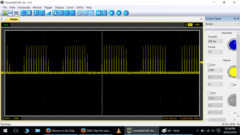
If any bad RAM address in this range is found it loops in the bad section, showing just 2 short IORQ pulses repeated regularly and giving the tested address on A8-A15 which can be measured out with the scope. First L is shown (lower address part), after H is shown on the second pulse (higher address part).

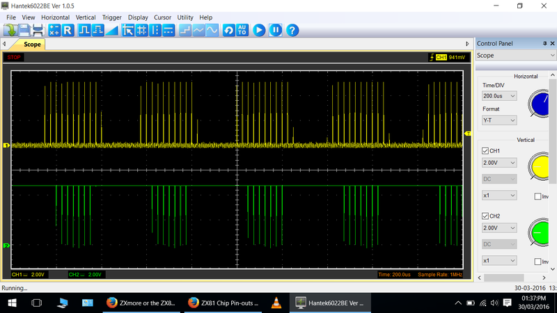
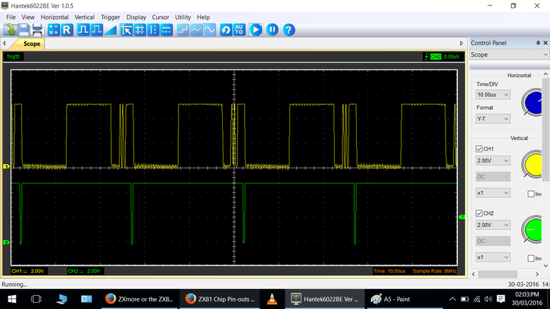
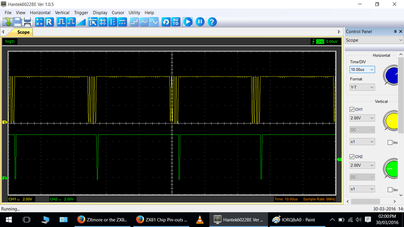
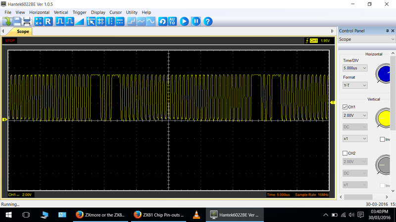
First part (after power-up in instance 3 with no key pressed):
IORQ (pin 20 of cpu) should be used as trigger signal and a second signal measured (triggering on falling edge).

IORQ one pulse every 33us with 400ns width (low pulse)
HALT, NMI high (no pulse)
WR with 10 low pulses between two IORQ pulses, nearly in the middle
A15, A13, A12 low (no pulse)
A14 with 11 high pulses between two IORQ pulses, the first and last half width of the other 9 pulses
A11 same as A14 but fast blinking, not steady
A10 same as A11 but blinking with double speed
A9 same as A11 but blinking with quadruple speed
A8 same as A11 but maybe blinking too fast to see it blinking (8 times speed)

RAMCS (pin 22 of RAM, IC3) with one single pulse, 9 double pulses, one single pulse (repeating)


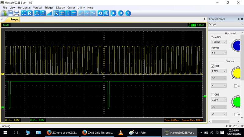
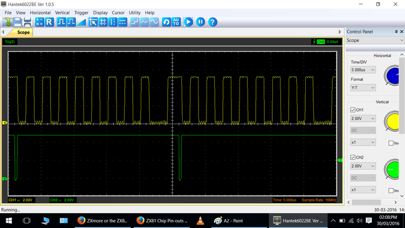
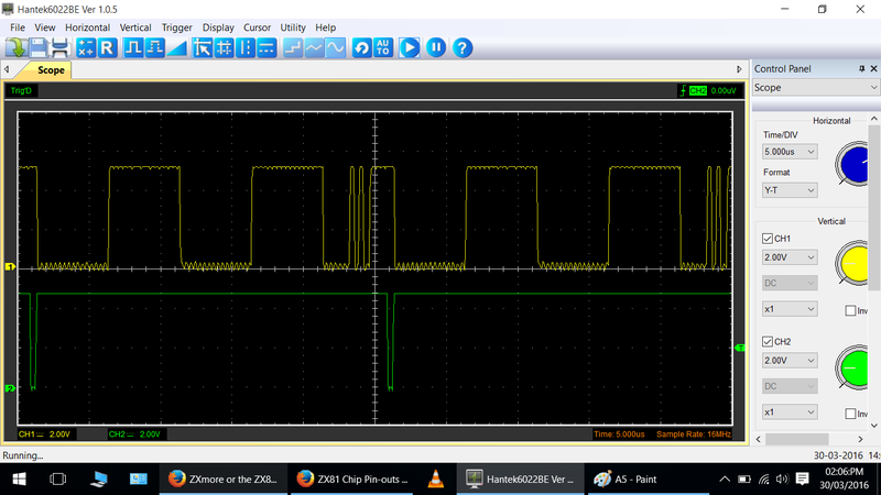
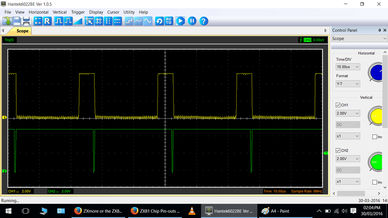
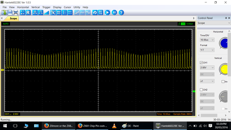
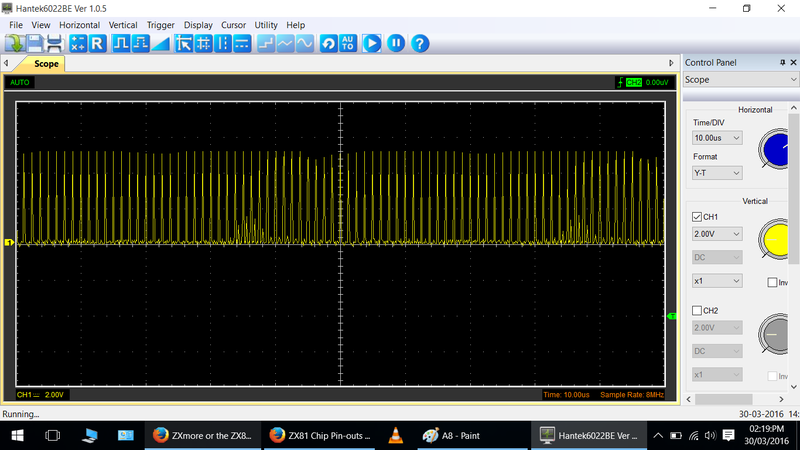
Second part (when shift key is pressed shortly):

The clk frequency changes from 6.5 MHz to 3.25 MHz as this code is interpreted to be video code (VIDON goes high, pin 11 of IC6) while it does not show a recognizable picture. So the above signals are still present with half frequency (IORQ pulse every 66us with 800ns width).

Additionally the following signals should be present:
Change trigger signal to A15 (pin 5 of cpu) with triggering on positive edge.

A15, A13, A12 two high pulses with 2us width directly followed, repeated every 16.6ms (maybe seen as one pulse depending on resolution)
VSYNC (pin 10 of IC11) - one high pulse repeated every 16.6ms, pulse width 60us, directly after the two single pulses on A12-A15

If these signals can be measured the access to the RAM should be working, also interrupts (INT) and keyboard IO.
This is for investigating deeper problems with an oscilloscope.
Attachments
ZXM-DIAG.zip
(39.4 KiB) Downloaded 212 times
User avatar
PokeMon
Posts: 2264
Joined: Sat Sep 17, 2011 6:48 pm

Re: ZXmore or the ZX80CORE follow-up

Post by PokeMon »

Lurch666 wrote:All of those signals have a gap as shown.
I am getting the 25us pulses but I just rechecked with the different frequencies and it shows regular gaps in the signal.
What could be causing that?
This is strange.
Could you test if you have any pulses at RESET (pin 26), WAIT (pin 24), BUSRQ (pin 25) ?
Do you have gaps in CLK with the same time resolution ?
User avatar
Lurch666
Posts: 36
Joined: Sun Nov 22, 2015 7:07 pm

Re: ZXmore or the ZX80CORE follow-up

Post by Lurch666 »

No pulses on those pins.they are all steady high except for the clk of course and that is a steady signal without gaps.
User avatar
PokeMon
Posts: 2264
Joined: Sat Sep 17, 2011 6:48 pm

Re: ZXmore or the ZX80CORE follow-up

Post by PokeMon »

Can you repeat and post a picture of IORQ and A15 (the first one) with a time resolution of 50us/div as there can not be seen quite much with the small needles. So just "one package" to investigate. I have not a specific idea now but A15 has to correlate exactly with IORQ and in the picture it looks like there are A15 pulses without IORQ which isn't possible with the correct working program.
Post Reply