xubuntu wrote: ↑Mon Nov 07, 2022 8:39 am
Will coral eprom work here or do we need to change things ?
No idea!
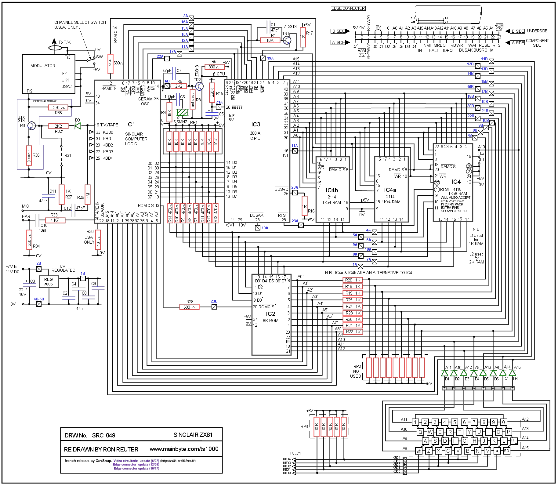
That diagram needs improving in my humble opinion.
A circuit schematic should be as clear and easy to read as possible. So mainly black on white rather than bright colours for starters. Only using colour to highlight very important items such as polarity or dangerous high voltages.
Using bus lines for data and address busses, with each signal line labelled where it splits out to go to a chip or component.
Other signal lines are normally shown as lines connecting to each component. Or where this is not practical, or would make the diagram difficult to read, the label should give both the signal name and the identity of the destination where it is going (e.g. /MREQ to IC7 pin 5) so that the reader does not have to search the entire diagram looking for it.
The layout should be spaced such that there is enough room to show components and connections without them being too close together or overlapping or on top of one another.
Each chip should be clearly labelled with a recognisable part number, long strange numbers that mean nothing to me are of no use. I can guess what each chip (strangely labelled as SK3, SK1 etc.) is, but that diagram does not actually say.
With regards to the ROM, which type of chip is it? Is it a mask ROM, a EPROM, a EEPROM, a flash ROM? And which size/capacity/version/make?
I don’t see an address line for A13 there, so it looks like it may only be a 8K byte type.
Although this diagram does not use bus lines for data and address busses, it is clear enough that it is reasonable enough to read without difficulty:
 Mark
Mark


